Brane Interface is a technology startup working to develop a low cost, compact and non-invasive brain-computer interface (BCI). We believe that BCI devices requiring brain surgery are a non-starter. Our BCI will be located in a pair of earbuds or integrated into a hat.
Using a single atomic layer of carbon called graphene, Brane Interface plans to link a human brain with an external device such a smartphone by sensing the faint magnetic fields of human thought. Medical applications of the technology include assisting those who have been paralyzed to gain control over robotic limbs using only their thoughts. Consumer applications include enabling people to interact with their smartphone/computer using thought commands in place of touch or voice interfaces.
Brane Interface has two proof-of-concept prototypes of its invention (two patents pending) that use a thin polymer membrane and a third prototype using a graphene membrane (the inspiration for “Brane”) that is transferred to a silicon-metal-oxide substrate. A fourth prototype using graphene along with several new substrate features to increase sensitivity is currently under development.
After completing a computer model using Math-Cad software, we set out to make a proof-of-concept prototype of our magnetic field sensor.

We made the first part of our sensor out of acrylic using a laser cutter.

Using an array of ultraviolet lights and UV-cure epoxy, we applied an aluminum-polymer membrane to our acrylic structure.

Our completed first prototype showed that we could measure an external magnetic field by sending a current through our conductive membrane and measuring a change in capacitance with a multimeter.
We decided to make a much smaller prototype using photolithography.
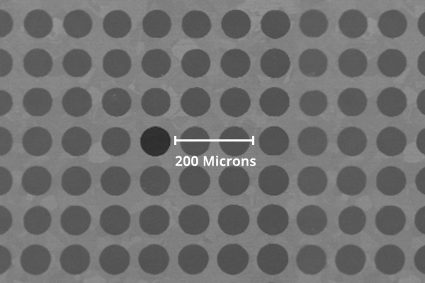
Etching an array of conductive membranes.

Using a spin coater to apply photoresist.

A single conductive membrane post etch.

A simple photomask used to make the conductive membrane of our sensor.

A flexible printed circuit board used as the sensor’s source, drain, gate and capacitive stator.
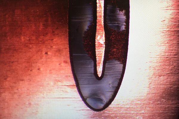
A close up view of an etched conductive membrane using an optical microscope.
Now it’s time to make a “real” device using a single atomic layer of carbon.

Searching for graphene using a scanning electron microscope or “SEM.”
Graphene membrane array captured in SEM.
A small feature on a silicon wafer to test a graphene membrane.

Loading a copper-graphene sample into the SEM.

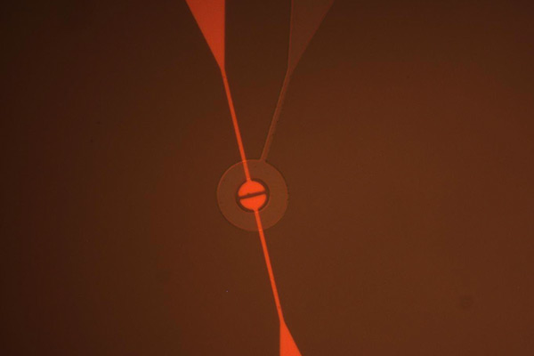
The basic operating principle of a graphene-based magnetic field sensor.
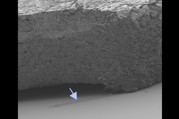
A SEM image of a small strip of graphene next to the edge of a business card. Graphene is really thin!

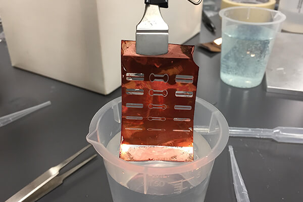
Searching through several copper-graphene samples to find the best ones.

Several copper-graphene “fly swatters” that are ready for transfer to a silicon-oxide-metal device.

Aligning and transferring graphene to a silicon-oxide-metal device.

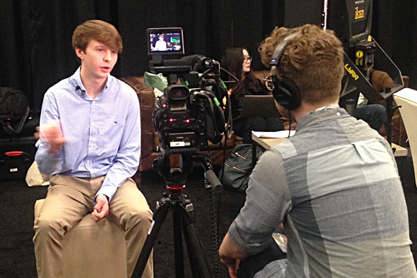
I met several really smart BCI researchers at my SXSW booth and learned a ton.

I still can’t believe I won the 2019 SXSW Innovation Award in my category!

Our equation above shows the importance of current density and membrane thickness.

Only graphene has the current density required to measure the faint magnetic fields of human thought.

Graphene is just one atom thick so it is much more sensitive than existing MEMS sensors.
I recently graduated Rice University with honors and will start graduate school at UT Austin in the Fall of 2025. In addition to developing novel BCI and clean energy devices, I also love to read about Roman history and make short films. After graduate school I think it would be fun to challenge tech’s “frightful five” with a series of BCI devices that offer a much more natural way to interface with the digital world. I also want to use the miraculous properties of graphene to lower the cost of clean energy devices.